Core point
Silicon wafers are important raw materials for the upstream of the semiconductor industry, accounting for about 40 % of the value of all semiconductor raw materials.at present,8 -inch and 12 -inch silicon wafers are the most mainstream silicon wafers, and demand will continue to migrate to large size.The barriers of semiconductor silicon wafers include: technical barriers, key materials and equipment barriers, customer certification barriers, funds and scale barriers, and talent barriers.
After 2020, the semiconductor silicon wafers entered the prosperity cycle, and the market size reached a record high, reaching $ 13.8 billion in 2022.The production capacity of mainland China has expanded rapidly, and the demand for domestic silicon wafers has increased. In 2022, the mainland market size reached 13.8 billion yuan.The global semiconductor silicon market is an oligopoly monopoly pattern, and the top five manufacturers account for 86.6%of the market share.
Mainland Chinese silicon wafers are at a critical stage of realizing domestic alternatives, and some head companies have initially appeared.Under the current geopolitics, the trend of localization of semiconductor silicon wafers is more obvious.Currently, many domesticThe 8 -inch/12 -inch production line has been put into production one after another, and is in the stage of production capacity climbing and customer certification.
1. Classification of semiconductor silicon wafers and industry barriers
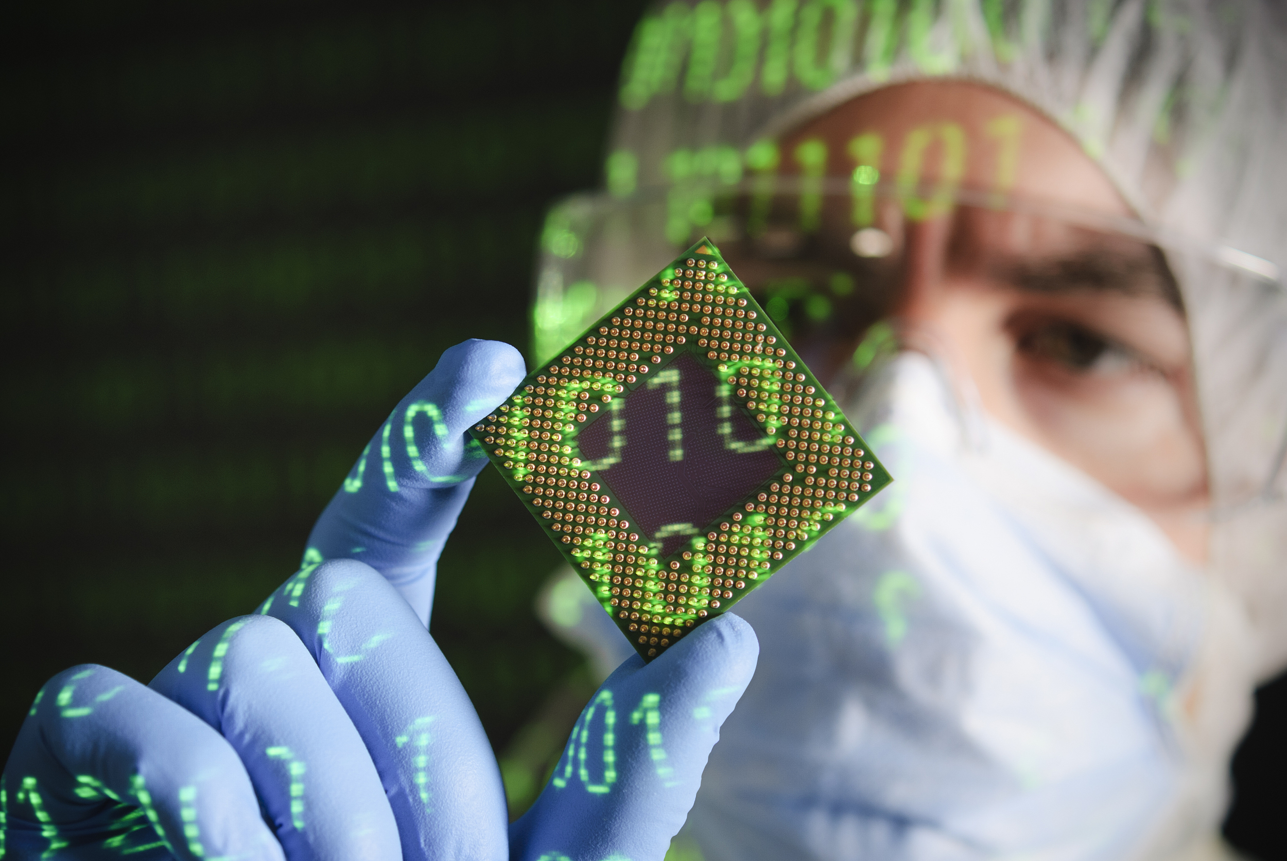
Silicon wafers are important raw materials for the upstream of the semiconductor industry. By conducting lithography and etching of silicon wafers, most semiconductor products can be created.At the same time, in the process of semiconductor manufacturing, the silicon wafer is the most proportion of raw materials, accounting for about 40 % of the value of all raw materials, and then electronic gas13%, 12%of the light cover, 12%of the photorettic glue, 7%CMP material, 6%wet chemicals, and a target of 2%.
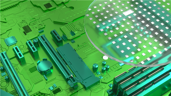
The purity requirements of semiconductor silicon wafers are high, the standard is11 or more (99.9999999999%) have extremely high requirements for crystal defects, surface flatness, smoothness, performance cleanliness, and impurities pollution.The semiconductor silicon wafer manufacturing process is complicated and there are many process links. The upstream electronic -grade polysilicon materials need to be purified and processing with a series of high technical thresholds such as stagry, grinding, polishing, and cleaning.Finally, the manufactured semiconductor silicon wafer wafers will be used for semiconductor manufacturing.
From the angle of size, the semiconductor silicon wafer product can be divided into4 inches, 6 -inch, 8 -inch, 12 inches and other specifications.The larger the size of the silicon wafer, the more difficult the manufacturing process, but the lower the cost of the unit chip, which is generally used in a more advanced semiconductor system.8-inch silicon wafers are mainly used to produce various types of MCUs, analog chips, sensors, power chips, radio frequency chips, etc.; 12-inch silicon wafers are mainly used for 28-90nm mature process and advanced processes below 28nm.Storage chip.
at present,8 -inch and 12 -inch silicon wafers are the most mainstream silicon wafers and the most important demand growth points.In 2021, the shipping area of 12 -inch silicon wafers accounted for 71%, 8 -inch silicon wafers accounted for 23%, and small size accounted for about 6%.From the perspective of trend, small -sized silicon wafers have a large cost advantage in the manufacturing of separate devices, and the future demand remains stable; the cost performance of 8/12 inch silicon wafers will increase with the maturity of the process.The penetration rate of inch silicon wafers will continue to increase.
From the classification of manufacturing process, semiconductor silicon wafers can be divided into grinding pieces, polishing tablets, fire -reducing tablets, outer extensions,SOI film.Among them, grinding tablets are the first silicon wafers obtained by a series of machining processes of polysilicon materials, which are often used for manufacturing dividing devices. Polishing sheets are made of polishing on the basis of grinding tablets.The substrate is used to produce degenerate films, outer extensions, SOI films, etc.Different types of silicon wafers are generally used in the production of different chip products, but there are also overlap applications.
Semiconductor silicon wafer leading enterprises have a relatively obvious first -mover advantage and scale effect, and the industry barriers are high:
The first is technical barriers.Semiconductor silicon wafers have high requirements on multiple indicators such as size, purity, and cleanliness, and have a high degree of technical professionalism. The process of each link needs to be accumulated for a long time.Especially with the continuous evolution of process and silicon wafers, the requirements for performance indicators and technical levels are getting higher and higher.
The second is the barrier of key materials and equipment.Electronic -grade polycrystalline is the most important raw material upstream of silicon wafers, occupying the cost of supporting materials25%.There are only a few manufacturers that can produce electronic -level polysilicon in the world that can produce electronics -grade polysilicon. There are still a few in Germany, South Korea, and the United States. At present, domestic manufacturers still rely on overseas manufacturers. However, domestic manufacturers have broken through high -purity mass production preparation technology, and the domestic rate has continued to improve.
The most critical of the production equipment of silicon wafers is single -crystal furnace and polishing equipment. It has long been monopolized by the United States, Japan, South Korea, and German manufacturers for a long time. Domestic equipment has made breakthroughs in critical links.Among them, single crystal furnaces are generally developed or extended by silicon film manufacturers, and it is difficult to buy equipment for domestic manufacturers.
Third, customer certification barriers.Semiconductor manufacturers have strict requirements on the quality of silicon wafers, very cautious about suppliers and high viscosity.Silicon film manufacturers need to go through more links and time to enter downstream customer suppliers. Generally, they need to be tested, tried, evaluated, and batch supplies downhill.3-5 years.
Fourth, funds and scale barriers.The semiconductor silicon wafer manufacturing process, high production equipment, and large investment in large -scale production and construction.For example, oneThe investment in the 8 -inch production line of 100,000 pieces/monthly capacity is 700 million yuan, and the 12 -inch production line investment of 300,000 pieces/monthly capacity is as high as 4.6 billion yuan.Due to the large investment investment, the low profit of silicon film manufacturers and high operating pressure in the early stage, it is necessary to make a certain scale before profitable.
Fifth, talent barriers.The R & D and production of semiconductor silicon wafers involves multi -disciplinary fields such as physics, thermodynamics, chemistry, and quantum mechanics, and composite talents with comprehensive professional knowledge are needed.At the same time, the various production technology knowledge of semiconductor silicon wafers needs to accumulate for a long time, and the same demand for experienced talents is also large.
2. Global market structure and development of domestic enterprises
Semiconductor silicon wafers are the key raw materials of the semiconductor industry. The market size is directly affected by the degree of prosperity of the semiconductor industry, which is also periodic.In 2018, the demand for semiconductor technology brought about by the development of new generation of information technology such as 5G, the Internet of Things, and smart cars broke out. The sales revenue of semiconductor silicon wafers exceeded 10 billion US dollars.After 2020, the epidemic impacted the global digital transformation accelerated, and the demand for the semiconductor industry was strong, driving the semiconductor silicon wafer to enter the prosperity cycle.
As the world's largest semiconductor consumer market, the wafer capacity has continued to expand.According to statistics, more than a quarter of the newly added wafer capacity in the past three years has come from mainland China.The expansion of the wafer plant and the continuous high production rate of capacity utilization have increased the demand for domestic semiconductor silicon wafers.In 2021, the semiconductor silicon film market in mainland China reached 11.9 billion yuan, an increase of 39%year -on -year, and exceeded the tens of billions of mark for the first time, and reached 13.8 billion in 2022.
In the market competition pattern, due to the high barriers of the semiconductor silicon wafer industry in terms of technology, capital, and scale, the global semiconductor silicon wafer market has basically formed an oligopoly monopoly pattern.63.8%, the top five manufacturers account for 86.6%.Among them, the market proportion of SHINETSU (SHINETSU) market accounts for 27.5%, Japan's Sumco (Sumco) market share is 21.5%, Taiwan ’s global wafer market share is 14.8%, Germany’ s Shichuang electronic market share is 11.5%, South KoreaThe market share of SK Siltron reached 11.3%, the market share of French SOITEC was 5.7%, and the market share of Shanghai Silicon Industry in mainland China was 2.2%.
Looking back at the development history of global silicon wafers, and the effective path of rapid development through mergers and acquisitions.Because the production of semiconductor silicon wafers has a strong scale effect, mergers and acquisitions can quickly achieve production capacity expansion.At the same time, manufacturers can improve market concentration, enhance the bargaining capacity of the industrial chain to maintain profitability.
Mainland Chinese silicon wafers are at a critical stage of realizing domestic alternatives. Some head companies have initially emerged and the competitive pattern is more intense.Under the current geopolitical and international trade environment, semiconductor silicon wafers are used as key raw materials for semiconductors, and the supply of localization is more obvious.
For example,In 2020, the Global WAils of Taiwan Silicon Film manufacturers in China acquired German silicon film manufacturers Shichun Electronics, but was eventually blocked by the German government in 2022.Therefore, mainland China semiconductor manufacturing enterprises have gradually selected domestic silicon wafers suppliers, and the localization space of silicon wafers is broad.Beginning in 2020, domestic manufacturers have begun to build a large -scale 8 -inch and 12 -inch semiconductor production line. At present, multiple production lines have been put into production, and they are in the stage of production capacity climbing and customer certification.
For more electronic conponents,please refer to:https://www.ciselec.com/en/products.html