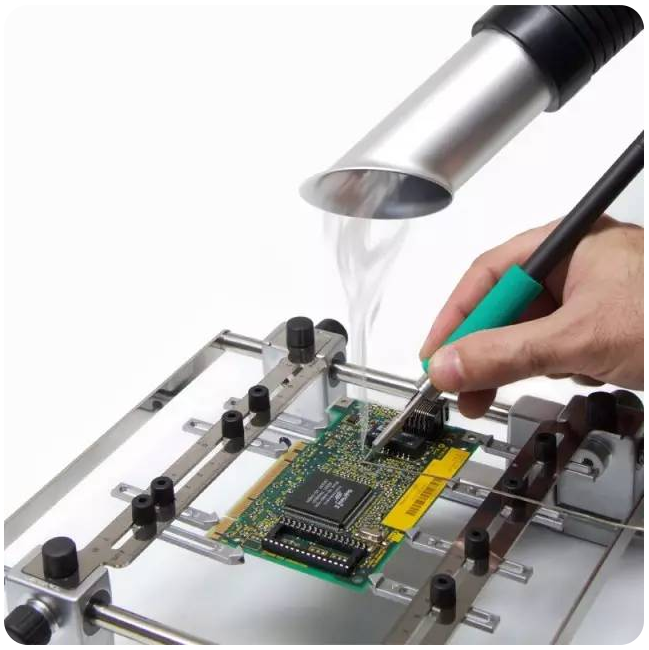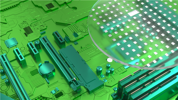
FPGA represents the on -site programming door array. In essence, FPGA is a set of interconnected digital sub -circuits that can achieve common functions and also provide very high flexibility. But it is necessary to fully understand FPGA. More subtle differences. This article introduces the concept behind FPGA, and briefly discusses what logical door is, how to program FPGA, and the difference between FPGA and microprocessors in design.
FPGA and microcontroller (or, microcontroller can be used, why use FPGA?)
Micro controller has become a leading component in modern electronic design. They are cheap and widely used. Now they are often used as a person's first introduction to the electronic world. We naturally continue to use the components we are familiar with, and as the microcontroller becomes stronger and stronger, there is no need to consider alternative solutions to cope with our design challenges. Nevertheless, the microcontroller is built around the processor. There are some basic restrictions in the processor. You need to recognize these restrictions. In some cases, these restrictions need to be overcome.
So, when will engineers choose FPGA instead of microcontroller? The answer is attributed to software to hardware.
The processor performs the task by performing instructions in order. This means that the operation of the processor is inherently limited: the desired function must adapt to the available instructions, and in most cases, it is impossible to complete multiple processing tasks at the same time.
The microcontroller is constructed around a processor, the processor is constructed around a CPU, and a CPU performs one operation at one time.
The instruction set is designed to be highly general, and the instructions can now be executed at a high frequency; however, these characteristics do not eliminate the shortcomings of software -based digital design methods.
Another choice is a method of hardware. If each new design can be constructed around a digital IC that realizes the function required by the system, it will be very convenient: there is no need to write software, no instruction set restrictions, no delay, only one input pin, output output, output, output The IC of the digital circuit corresponding to the accurate operation of the pin and the necessary operation. This method is unrealistic because it needs to design an ASIC (special integrated circuit) for each circuit board. However, we can use this method to use FPGAS.
What is the on -site programming door array?
A good name can provide a lot of information. I think the "on -site programming door array" is a very good name. FPGA is a logical door array (eh, it is considered to see below), this array can be the program program (in fact, "configuration may be a better word) People come to complete. Let's take a closer look at these basic characteristics.
Logic doors (with, or, different, etc.) are the basic components of digital circuits. Therefore, a digital device designed to achieve high configuration (that is, "on -site programming") consists of many custom -made ways. It is not surprising.
However, FPGA is not a huge collection of a single Boors. This will be a very good way to provide configurable logic functions, because it does not use such a fact, that is, public operations can be achieved as a fixed module more effectively. The same principle is also obvious in the field of separate digital ICs. You can buy ICs composed of door, or door, but you don't want to use a single door to build a displacement register. Instead, you will buy a shift register integrated circuit.
Therefore, FPGA is not just a door array. This is a series of carefully designed and interconnected digital sub -circuits that can achieve common functions efficiently while providing extremely high flexibility. Digital subcourse is called configurable logic module (CLB), which constitutes the core of FPGA programming logic function:
CLB needs to interact with each other and interact with external circuits. For these purposes, FPGA uses a programmable interconnection matrix and input/output (I/O) module. FPGA's "program" is stored in the SRAM unit, affecting the function of CLB, and controlling the establishment of a connection path.
Detailed explanation of the internal structure and operation of CLB requires a whole article (if it is not multiple articles). The general idea is that the CLB includes a multi -way reusrator that searches tables, storage elements (triggers or registers), and allows CLB to perform Boolean operations, data storage and arithmetic operations.
The I/O module consists of various components to facilitate communication between CLB and other components on the board. These devices include pull/drop -down resistor, buffer and anti -phase device.
On -site programming logic (or in other words, how to program FPGA?)
How do we turn a CLB array into a digital circuit and make it accurately complete the function we want? At first glance, this seems to be a quite complicated task. In fact, FPGA is often considered more difficult than micro -controller programming. However, FPGA development does not need to completely understand the CLB function or internal interconnect, just as the micro -controller development does not require a thorough understanding of the processor's assembly language instructions or internal control signals.
In fact, FPGA is misleading as an independent component. FPGAS is always supported by development software, and the software executes the complex process of transforming hardware design into a programming position that determines the programming position of interconnection and CLB behavior.
Hardware description language
People have created language so that we can "describe" hardware; they are called (very appropriate) hardware description language (HDLS), the two most common are VHDL and Verilog. Although there are obvious similarities between HDL code and the code written in advanced software programming language, the two are fundamentally different. The software code specifies a series of operations, and the HDL code is more like a schematic diagram. Using text to introduce components and create interconnection.
in conclusion
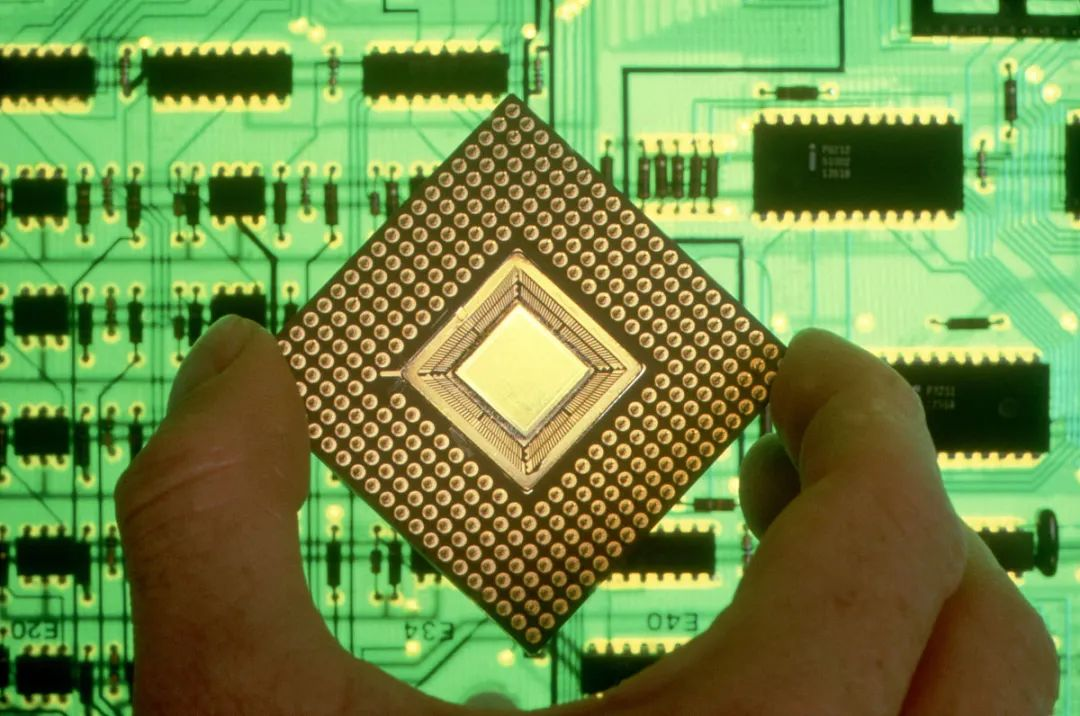
The basic characteristics of programming logic devices and the potential advantages of the system of the processor -based system. Hyundai FPGA is a complex high -performance device. It may be a bit daunting for those who are accustomed to collecting data, control ASIC and performing mathematical operations. However, it may be found that in certain applications, the improved performance and multifunctionality are worthy of design work.
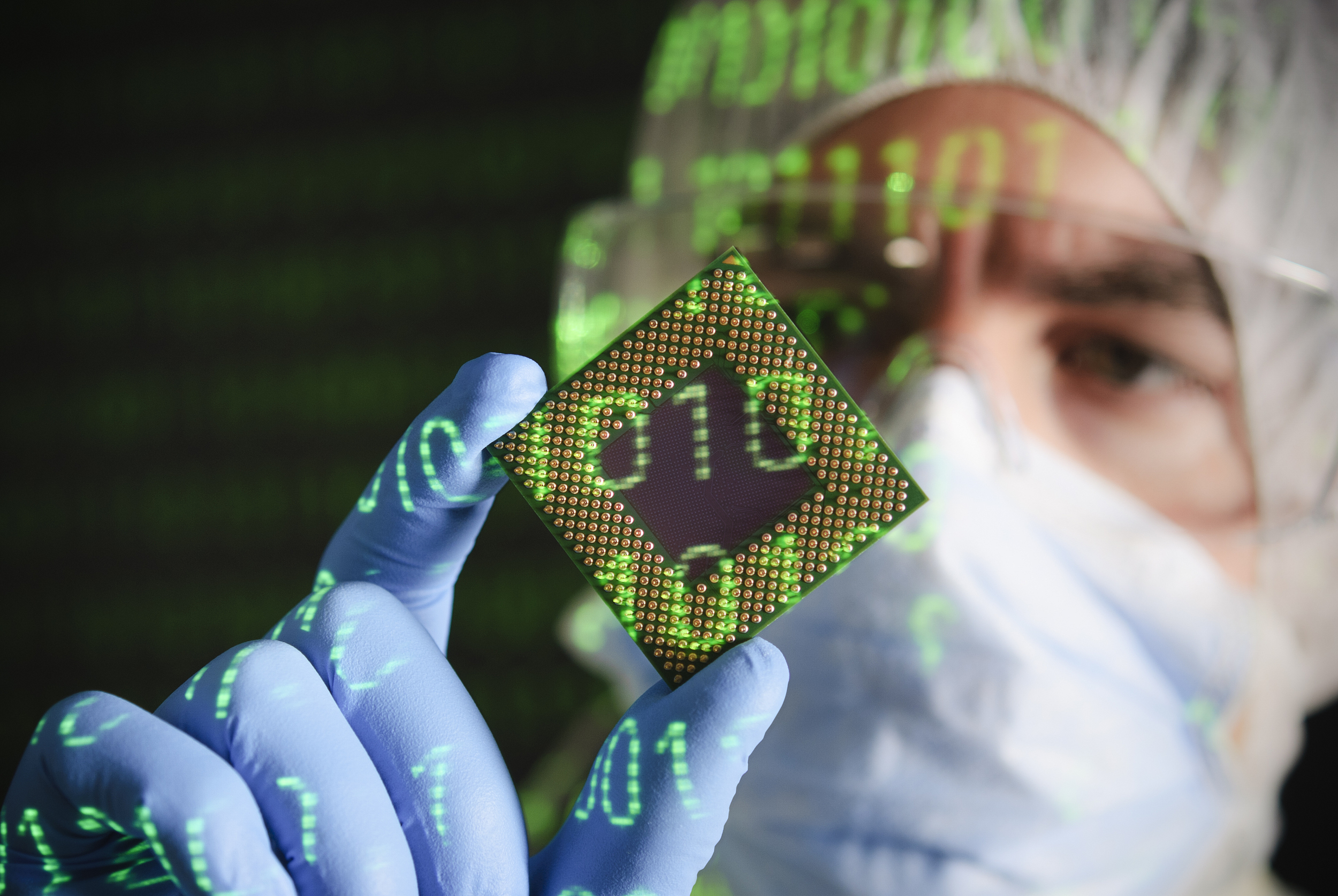
resolution, stability and anti -interference ability of the identification system. At this point, the virtual Digital Technology proposes the high -precision application of deep learning algorithms in the visual of the machine. In this context, the DLIA industrial defect detection plays a decisive role.
The DLIA industrial defect detection By constructing a deep neural network model, the system can automatically learn and extract features from massive training samples, thereby achieving precise identification of complex and fine characters on the chip surface. Even in the face of image quality fluctuations caused by light change, angle deviation, or surface reflection, deep learning algorithms can be quickly adapted and made accurate judgments.
With the deep fusion of machine vision and deep learning, the degree of automation and accuracy of chip surface character recognition has been greatly improved, significantly improved production efficiency, reducing human error risk, and providing details for subsequent product quality management and process optimization of process optimization. Reliable data support.
This deep learning -enabled machine visual technology breaks through the limitations of traditional character recognition in accuracy and speed. Even the most subtle scratches, pollution or deformation can be discovered and recorded in time, which greatly improves the level of surface quality control level It effectively reduces the rate and repairs in the production process.
The surface character recognition of the chip, as an important application scenario of machine vision technology in the microelectronics manufacturing industry. With its excellent performance of fusion and deep learning, it has become one of the key driving drivers for the high -quality development of the industry. New era of industrial quality inspection.
For more electronic conponents,please refer to:https://www.ciselec.com/en/products.html