1. Design and mask production
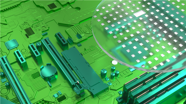
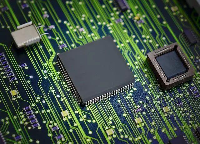
This process starts with chip design. The engineer creates a detailed layout design to specify the placement and interconnection of transistors, resistors and other components. The engineer will use the design to create a mold cover as a template that defines the pattern on the semiconductor wafer during the manufacturing process.
2. Worse preparation
The engineer uses silicon wafers as a substrate to undertake the task of polishing and cleaning to eliminate any impurities. Next, a thin layer of oxidation layer will be formed on the surface of the silicon wafer. It provides a smooth and uniform starting point for subsequent process steps. By controlling the formation of the oxidation layer, it can ensure the physical and chemical characteristics of the need, and provide a good foundation for subsequent deposition and pattern transfer.
3. Light carvings
During the light engraving, engineers will use the previously created mask to complete the key image transfer steps. First of all, they apply a layer of light glue on the wafer surface and place the mask on the lithography glue. Subsequently, through a specific light source and lens system, the pattern on the mask was exposed on the optical glue on the wafer surface. This exposure process makes the pattern on the mask be accurately transferred to the light glue.
Next, selectively remove the exposure or unre exposed area through the development steps. After the development, the pattern on the lithography glue is retained on the wafer surface, providing accurate guidance for subsequent etching and material removal steps.
4. Captive
The etching is used to remove the material from the wafer that has been selectively removed. In order to create the required patterns, engineers use a variety of different etching processes to handle different materials, such as silicon, polysilicon and metal layer. By accurately controlled the etching process, the material can be ensured accurately, thereby forming accurate patterns and structures.
5. deposits
Chemical gas deposition (CVD) or physical gas sedimentation (PVD) and other technologies have deposited thin films (such as metal or insulating layers) on the surface of the wafer surface. These sedimentary layers form the conductivity, insulation layer and other components of semiconductor devices.
6. ion injection
This step involves a specific area where the doping agent is introduced into the wafer to change its electrical performance. Ion injection is incident with a certain energy -scale ion beam. A series of physical and chemical interactions occur with the atoms or molecules in the material, which changes the surface component, structure and performance of the material, so as to optimize the surface performance of the material, or obtain a certain certain Some new excellent performance. Ion injection is essential to generate the required transistor characteristics.
7. Enemies
After the injection phase of the ion is injected, the wafer will be treated with high temperature annealing. The main purpose of this step is to activate any structural damage caused by doping agents and repair the injection process. Through annealing treatment, the defects caused by ionic injection were repaired, and the integrity of the wafer was restored, laying the foundation for subsequent manufacturing steps.
8. Chemical mechanical polishing (CMP)
CMP is responsible for ensuring the smoothness and uniformity of the wafer surface. The main task of this step is to eliminate any protruding or depression on the surface and create a smooth and uniform surface. A smooth and uniform surface can reduce defects, improve electrical performance, and enhance long -term stability reliability of semiconductor devices.
9. Measurement test
During the semiconductor manufacturing process, engineers will conduct a series of measurements and inspections to ensure that each step meets the required specifications and standards. This involves the use of highly accurate and complex tools to check the size, layer thickness, material purity, and other key parameters. The accuracy of measurement and inspection is essential for creating high -performance and reliability semiconductor devices.
10. Packing
Finally, come to the packaging and testing session, and prepare for distribution and use. Packaging is a key step to protect the chip from environmental impact, and at the same time, it is necessary to ensure that its electrical and thermal performance meets the design requirements. With the continuous progress of technology, the packaging process is also developing to meet the needs of smaller and high -performance semiconductor devices.
For more electronic conponents,please refer to:https://www.ciselec.com/en/products.html

