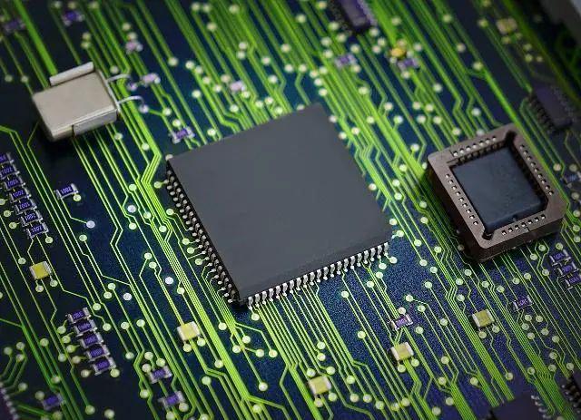
1、Silicon wafer
The silicon wafers are located in the upstream of the semiconductor industry chain. They are the main raw materials of semiconductor devices and solar cells. They are mainly used in two areas of photovoltaic and semiconductors. The downstream demand has continued to grow in recent years. From the perspective of in the field, the production capacity of photovoltaic silicon wafers is mostly concentrated in my country. Leading companies such as Central and Longji have strong strength, and the production technology level is the world's leading.
For photovoltaic silicon wafers for photovoltaic silicon wafers, the production process is more complicated, the application scenarios are more, and the market value is higher. The mainstream 12 -inch silicon wafers in the market have not yet reached large -scale production in my country, and they are seriously dependent on imports. Domestic companies represented by Shanghai Silicon Industry are trying to break the technical barriers and have a wide range of domestic replacement space.
(1) Wide in the downstream application of silicon wafers, is an important material for semiconductor devices and photovoltaic batteries
Silicon is a good semiconductor material. It has good high temperature resistance and good radiation resistance. It is particularly suitable for making high -power devices. With silicon as the raw material, a silicon rod is made by pulling single crystal, and then cutting is formed to form a silicon wafer. Silicon wafers are mainly used in the two major fields of semiconductor and photovoltaic. Semiconductor silicon wafers are higher than photovoltaic chips in aspects of crystals, shapes, size, and purity. (99.99%-99.9999%), semiconductor silicon wafers are about 9N-11N (99999999%-99.99999999%). The production process is more complicated and the downstream applications are more wide.
Semiconductor silicon wafers are located at the top of the industrial chain. They are mainly used in integrated circuits, separate devices and sensors. They are key materials for manufacturing chips. They affect the development of lower -reaches automotive and computers and other industries. It is the cornerstone of the semiconductor industry chain.
(2) Photovoltaic silicon wafers: China's production capacity is leading, leading enterprises are strong
The photovoltaic industry is one of the national strategic emerging industries. Photovoltaic silicon wafers are located on the upper reaches of the photovoltaic industry chain. In recent years, its demand is rising. According to CPIA forecasts, the global photovoltaic market volume will reach 150GW in 2021. It has a wide range of vastness. Market and development prospects.
my country is the world's largest producer of photovoltaic single crystal silicon wafers in the world. According to the statistics of the China Nonferrous Metal Industry Association Silicon Branch, as of the end of 2019, my country's single crystal silicon wafers have 115GW, accounting for 97.6%of the world's. Leading enterprises Longji and Central occupy more than 50%of domestic single -crystal silicon wafers, and in the process of continuous expansion production capacity, new forces companies have also accelerated production and expanding production.
According to the company's communiqué statistics in 2020 my country's single crystal silicon wafers will be about 190GW, and it is expected that the domestic single crystal silicon wafer production capacity will reach 240GW by the end of 2021.
(3) Semiconductor silicon wafers: serious dependence on imports, and domestic alternative space is broad
Benefiting from the technological progress of semiconductor products and the increase in the category of downstream -related electronic consumer products, the demand for semiconductor silicon wafers has increased year by year, and the scale continues to increase. The scale of the global silicon wafer market in 2020 will reach about $ 11 billion, and the market prospects of semiconductor silicon wafers will be broad.
Due to the high technical barriers of semiconductor silicon wafers, the global semiconductor silicon wafers are monopolized by giants today, with high concentration, and manufacturers in mainland China are small. In 2020, the top five global silicon wafer providers, SHIN-ETSU, Sumco (SUMCO), GlobalWafers, Taiwan, Silitronic, and SKSILTRON The market share of more than 80%, the market share of Shanghai Silicon Industry, local manufacturers in my country, is about 2.2%, and the volume is small.
The larger the size of the silicon wafer, the higher the production efficiency of the unit wafers. Since the 1970s, the silicon wafer has developed in a large size. Today, the largest mass -produced silicon wafer size in the world today is 300mm, which is a 12 -inch silicon wafer. The demand for 12-inch wafers has risen in recent years. According to Japan's victory, the CAGR of 12-inch wafers can reach 5.1%from 2020-2024. Global semiconductor silicon wafers are mainly concentrated in industry giants. my country ’s semiconductor silicon wafers start late and have a backward development. Only a few companies have 200mm (8 -inch) silicon wafer productivity. my country’ s 12 -inch silicon wafers All depend on imports.
Making large silicon wafers has high purity requirements for silicon, and also has very high requirements for the processing process of chamfering and precision grinding. my country's technology level is backward, and the large -scale production of 12 -inch silicon wafers has not been achieved. In 2018, the Shanghai Silicon Industry achieved a large -scale sales of 12 -inch silicon wafers, breaking the situation of 0 large -sized silicon wafers. The 12 -inch silicon wafers are still the mainstream of the silicon wafer market today. Domestic manufacturers have the opportunity to catch up. The domestic alternative of large -sized silicon wafers still has a large space.
In order to promote the localization of the important material of semiconductor silicon wafers, the Chinese government has also introduced a series of policies to support industrial development, promote the research and development of large -sized silicon wafers, and promote the development of the semiconductor industry.
(4) Important listed companies
The business scope of domestic silicon wafers is widely covered, and photovoltaic and semiconductor silicon wafers are often involved. The leading enterprise of photovoltaic silicon wafers is strong in Central and Longji, and the leading leadership is stable; domestic manufacturers of semiconductor silicon wafers are accelerating the catch -up. Companies such as ultra -silicon semiconductors have also entered the field of large silicon wafers.
China is the world's largest semiconductor terminal market. With the continuous expansion of Chinese chip production capacity, the market size of my country's semiconductor silicon wafers will accelerate, and the development prospects of large silicon wafers are broad.
2、silicon carbide (SIC)
Silicon carbide is the third -generation semiconductor material. It has very superior performance and is an important raw material for power devices. In recent years, countries have invested a lot of human and material resources to develop related industries. The threshold of the silicon carbide industry is relatively high, and my country's production technology level is relatively backward. At present, the industrial structure presents the characteristics of the United States. Only Cree's company occupies 62%of the global share of silicon carbide chips.
The development prospects of the silicon carbide market have been widely developed. In recent years, it has continuously infiltrated in the fields of electric vehicles, photovoltaic, rail transits, and smart grids. It has strong downstream demand and the market size has continued to expand. my country is also layout of the entire silicon carbide industry chain. The number of relevant patents has continued to rise this year. big.
(1) The third -generation semiconductor material, new energy and 5G cornerstone
Silicon carbide is currently the most mature wide -forbidden band semiconductor material, and it is also a representative material for the third -generation semiconductor material.
Silicon carbide materials have many advantages: stable chemical performance, high thermal conductivity, small thermal expansion coefficient, wear -resistant high pressure. Products with silicon carbide materials can reduce the volume of 50%and reduce energy loss by 80%compared with products with the same electrical parameters. Due to these characteristics, countries around the world attach great importance to silicon carbide materials. Masters on the major semiconductor giants have also invested heavily in developing silicon carbide devices.
With the maturity of technical technology and the decline in preparation costs, it has been applied to various power devices. In recent years, the penetration rate of silicon carbide power devices has continued to rise in the field of new energy vehicles. Important raw materials.
(2) Europe and the United States occupy the key location of the SIC industry chain
The silicon carbide production process is divided into three major steps: single crystal growth, extension layer growth and device manufacturing, corresponding to the three major links: industrial chain base, extension, device and module. There is a high technical threshold in the silicon carbide industry.
It has a long period of R & D time. The United States, Europe, Japan and other countries and regions have continuously improved the preparation technology of silicon carbide single crystals and related equipment for research and development and manufacturing. Big advantage.
(3) The development of new energy vehicles and photovoltaic industries promotes the growth of silicon carbide market
Silicon carbide is an ideal material for extreme power devices. It is resistant to high temperature and high pressure, high energy conversion efficiency, and broad application fields. At present, there are four main application scenarios in silicon carbide power devices: 1) New energy vehicles: main inverters in the motor drive system; 2) photovoltaic: photovoltaic inverter; 3) rail transit: power semiconductor device; 4) smart grid) smart grid) smart grid) : Solid -state transformer, flexible AC transmission, flexible DC transmission, high -voltage DC transmission and power distribution system.
With the further development of silicon carbide power devices, its penetration rate in various fields has continued to increase. According to YOLE, the market space of global vehicle SIC power devices is expected to reach 1.93 billion US dollars by 2024, corresponding to the compound growth rate of 2018-2024 compound growth rate Reacked 29%. According to the Forecast of Tianda Henda Prospectus, the proportion of silicon carbide power devices in photovoltaic inverters will reach 50%in 2025, and the proportion of silicon carbide devices in rail transit will gradually increase.
Driven by the demand for electric vehicles and photovoltaic inverters, according to OMDIA forecast, emerging markets of silicon carbide and nitride power semiconductor are expected to exceed $ 1 billion in 2021; according to IHS Markit data, the size of the silicon carbide power device market in 2018 About 390 million US dollars, benefiting from the growth of new energy vehicle demand and the development of the photovoltaic industry. It is expected that the market size of silicon carbide power devices will exceed US $ 10 billion by 2027, and the growth momentum of the silicon carbide industry will be sufficient.
(4) The demand for silicon carbide is strong, and the industrial system is gradually deployed
my country is the largest application market for silicon carbide, but at present, my country's silicon carbide industry is still very incomplete. Most of the domestic research and development and manufacturing of silicon carbide materials and power devices are mostly research and development and manufacturing, and lack of large -scale production capabilities.
At present, China has a low market share in the field of silicon carbide, but it has gradually cultivated all aspects of the industrial chain, which is expected to achieve better development. The state also attaches great importance to the development of the industry. It promotes its development through the 863 plan and the National 02 major special projects, and includes silicon carbide substrates in the 13th Five -Year "Strategic Emerging Industry Key Product Catalog".
3、High -pure metal sputtering target
Splane targets are one of the core materials of integrated circuits. In recent years, it has developed towards the direction of high splattered and high -pure metals. Its downstream application scenarios mainly include semiconductors, panels, and solar batteries. With the development and improvement of the consumer electronics terminal market, the downstream demand of high-pure metal sputtering targets has continued to rise. The compound growth rate of the global target market in 2013-20202020 As soon as 14%, the market size gradually expanded.
The industry has high barriers to sputtering targets. The United States and Japanese companies have core technologies and monopolize the global market. my country's sputtering target industry starts late and is relatively backward, but its market demand is the world's leading worldwide, and domestic alternative space is large. Domestic enterprises are gradually breaking through the technical bottlenecks and strive to break the unfavorable situation of the US -Japan monopoly high -end target market.
(1) The core material of the integrated circuit
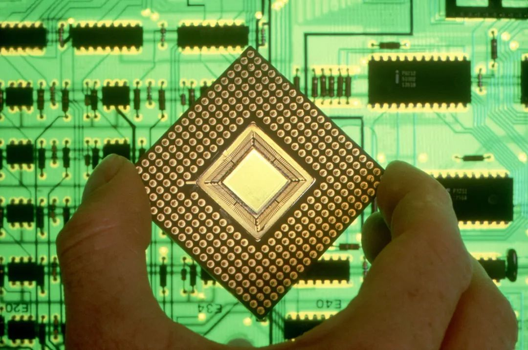
Splane is one of the important technologies for preparing film materials. Splash refers to the use of ions generated by the ion source to form a high -speed ion beam flow after accelerating the agglomeration in vacuum. Exchange, the atoms on the solid surface leave the solid and deposit on the base surface. The bombarded solid is the raw material of the sputtering method with a sputtering method, which is called sputtering target. In the integrated circuit, the medium layer, conductor layer and even protective layer of the unit device must use sputtering coating process.
Ultra -high -pure metal and sputtering targets are an important part of electronic materials. The sputtering target industry chain mainly includes metal purity, target manufacturing, sputtering coating, and terminal application. The target manufacturing and sputtering coating link is a key link in the entire sputtering target industry chain. It has high requirements for process levels and high entry barriers. The target is now developing towards the direction of high splattered sputtering rate, grain crystal control, large size, and high -pure metal. At present, the main high -purity metal sputtering targets include aluminum targets, titanium targets, pupa targets, tungsten titanium targets, etc., which are the core materials for preparing integrated circuits.
(2) Consumer electronics promotes the scale of the target market to expand
Downstream production of high -purity sputtering target products
The industry's market capacity has gradually expanded in recent years: 1) Semiconductor industry: With the continuous growth of semiconductor demand in the field of terminal consumption in the terminal consumption of smartphones and tablets, the capacity of the semiconductor market has further increased, and there are many types of sputtering targets in the semiconductor industry.
Large amount, stable downstream market growth will effectively promote the growth of sales scale of sputtering targets; Tablet display industry: In recent years, LCD display has gradually become the world's mainstream display technology, and it has gained a wide range of display markets in the plane display market. application. In order to ensure the uniformity of the large -scale membrane layer of the flat display, the sputtering technology is increasingly used to prepare these membrane layers.
Since the 1990s, the rapid development of the terminal application market such as consumer electronics has promoted the development of the high -purity sputtering target industry, and the market size has grown at a high speed. From 2013-2020, the global splash target market size is expected to rise from US $ 7.56 billion to 19.563 billion US dollars, with a compound growth rate of 14.42%
(3) The development and production of high -end targets are mainly concentrated in the United States and Japan
Famous foreign target companies have precipitated for decades in terms of target development and production. Globally, the number of enterprises participating in all aspects of the sputtering target industry chain is basically distributed in pyramids. The technical threshold of high -purity sputtering target manufacturing links, large equipment investment, and relatively small number of enterprises with large -scale production capacity. Distributed in the United States, Japan and other countries and regions.
(4) High -end targets have strong domestic demand, and domestic alternative space is large
According to estimates, domestic demand in 2019 accounted for more than 30%of the global target market, while local manufacturers supply about 30%of the domestic market. High -end targets are mainly imported from the United States, Japan and South Korea. The domestic target market has at least ten times the import alternative space. Essence
In terms of semiconductor user targets, according to statistics from the China Electronic Materials Industry Association, the domestic semiconductor market size was 1.615 billion yuan in the domestic semiconductor field. It is estimated that by 2025, the market size of domestic wafer manufacturing will increase to US $ 217 million, and the use of sputtering targets in the packaging field will increase to US $ 118 million, totaling 335 million US dollars, about RMB 2.345 billion Essence
Affected by the historical and technological restrictions, my country's high -purity sputtering target industry has started late. It is still a newer industry. The main high -purity sputter target manufacturers are invested by state -owned capital and a few private capital. Compared with the sputtering target produced by internationally renowned enterprises, there is still a considerable gap in the production level of Chinese sputtering targets, and the market influence is very limited. The country promotes the development of the industry through various policies.
The "Guidelines for the Development of the New Materials Industry" released in 2016 proposed that it is necessary to strengthen the research and development of high -purity metal sputtering target production technology. At the end of 2018, the tax exemption period of imported targets ended, and the possibility of opening domestic targets for domestic targets.
At present, the country is gradually breaking through the threshold for key technology and breaking the core technology of sputtering target material the US -Japan monopoly and products need to be imported backward. At present, some products of target manufacturers in China have reached the international advanced level, and the quality of product quality has been recognized by domestic and foreign downstream enterprises. By building factories near the downstream enterprise factories, the price of target materials may be 10%-15%lower than foreign manufacturers. The necessity and strategic significance of replacement are obvious.
For more electronic conponents,please refer to:https://www.ciselec.com/en/products.html